

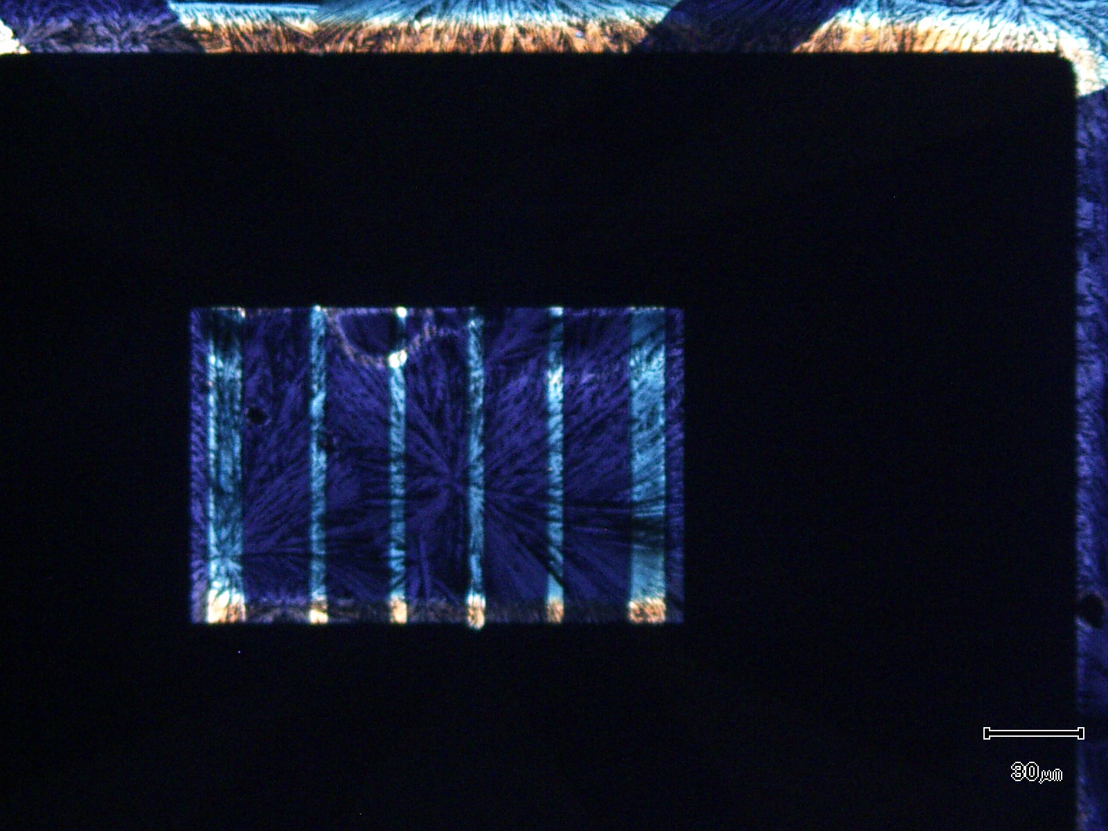

Optical microscopy image of the selective deposition of semiconductor crystals on a chemically modified substrate. The treated regions inhibit crystal growth, while in the transistor channel the semiconductor crystals grow, forming a polycrystalline layer. This contrast between hydrophobic and hydrophilic properties induces a well-defined pattern, relevant for the development of printed electronics, where wettability and capillary forces govern the formation of semiconductor layers.
-
Date: 06 May 2026
-
Hits: 31