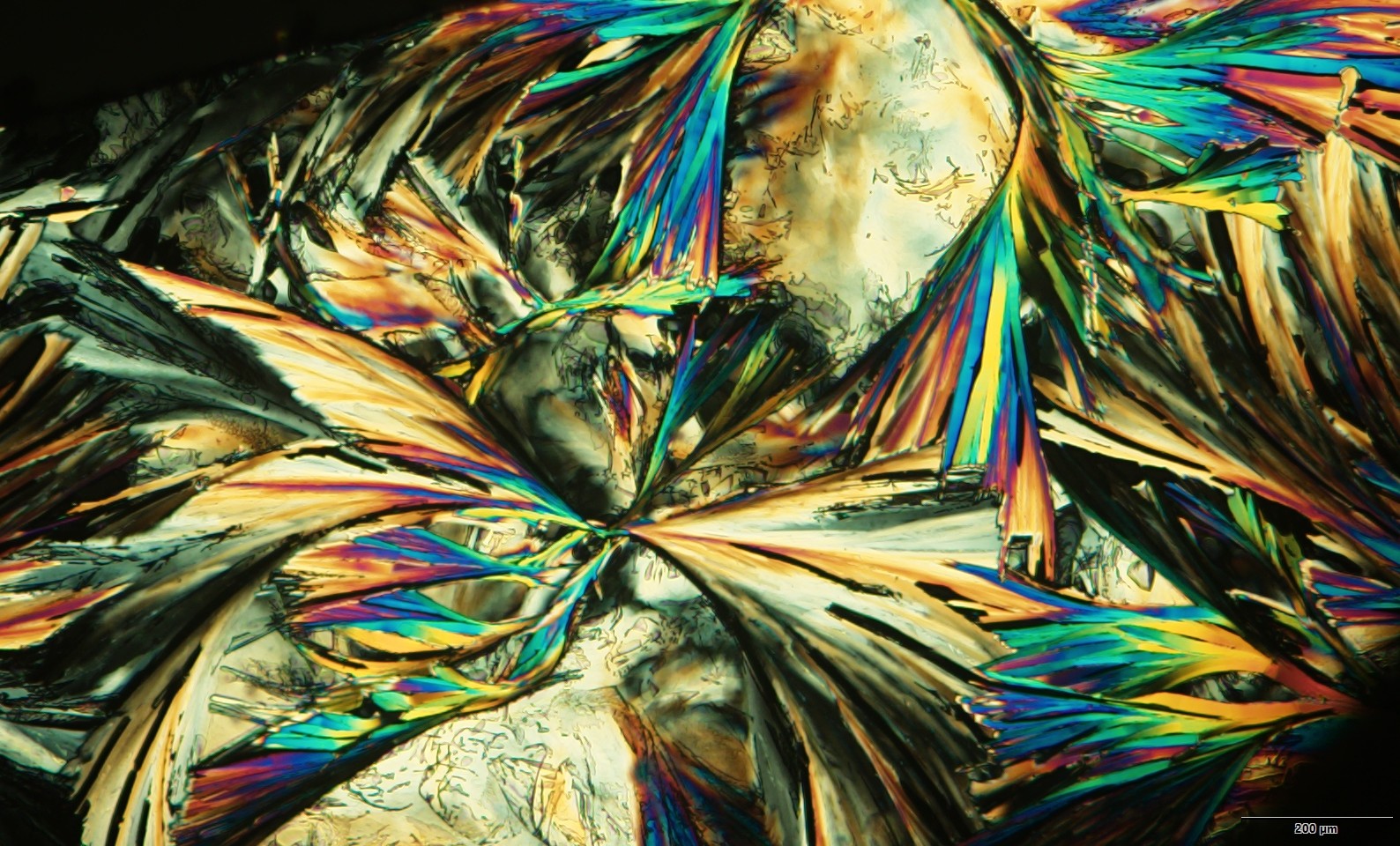
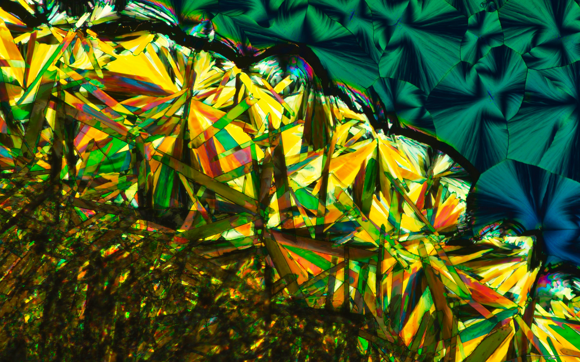
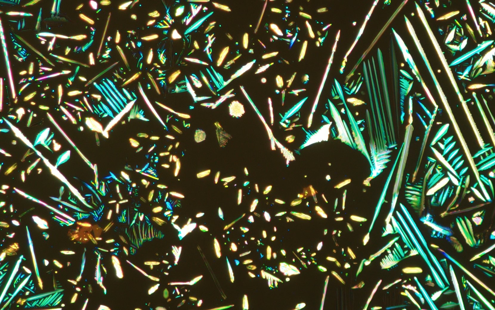
A polarized light microscopy view of a mixture of an azobenzene compound and a Phase Change Material. What looks like a stained-glass window or bird feathers is actually the microscopic world of energy storage. Such blends are key to developing "smart" thermal energy storage systems with light-responsive properties.
This image reveals the mosaic-like crystalline domains formed within a mixture of Azobenzene and a Phase Change Material. Using polarized light, the geometric boundaries show where different crystal orientations meet during solidification, showcasing the beautiful complexity found in materials science research
Optical microscopy image of the selective deposition of semiconductor crystals on a chemically modified substrate. The treated regions inhibit crystal growth, while in the transistor channel the semiconductor crystals grow, forming a polycrystalline layer. This contrast between hydrophobic and hydrophilic properties induces a well-defined pattern, relevant for the development of printed electronics, where wettability and capillary forces govern the formation of semiconductor layers.
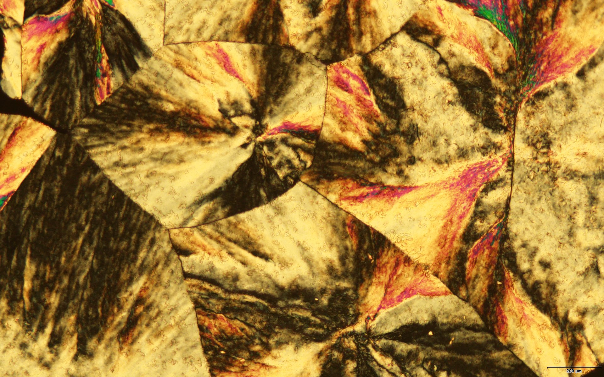
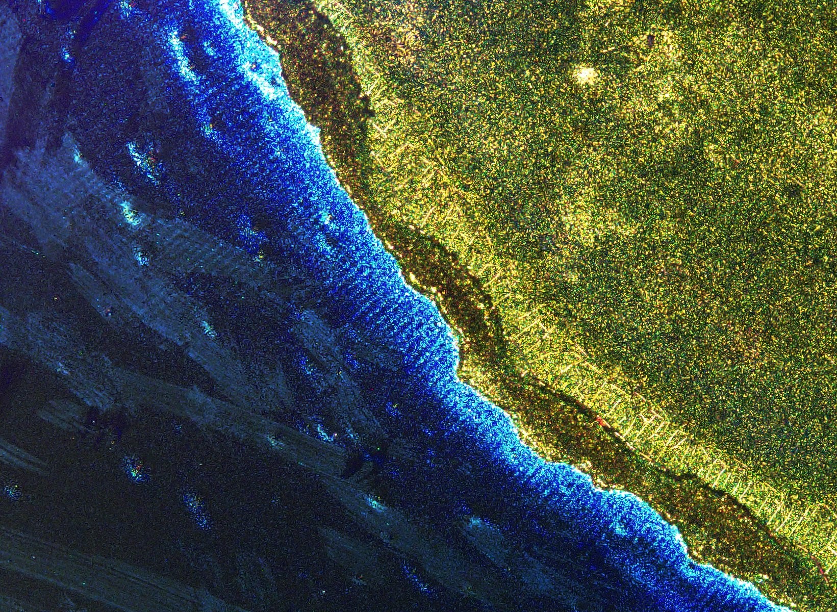
Imagen obtenida con microscopio óptico con luz polarizada que muestra estructuras cristalinas con morfología floral en tonos azules y patrones simétricos formados tras el tratamiento térmico de los films preparados desde disolución.
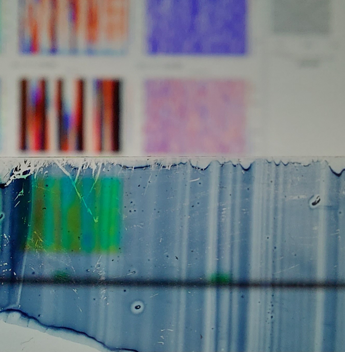
A microscope slide with a sample of an organic material used in solar cells with a spectroscopic image of the sample in the background.
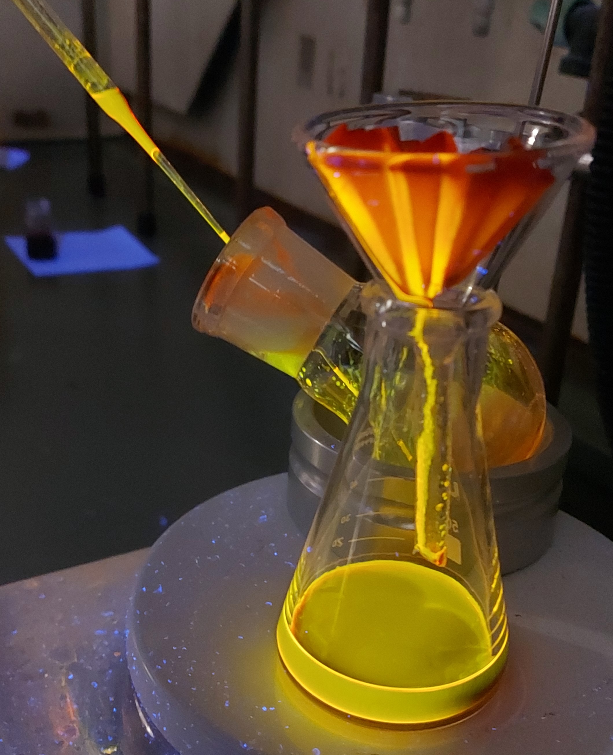
An organic functional material that is fluorescent being filtered while illuminated with UV light.
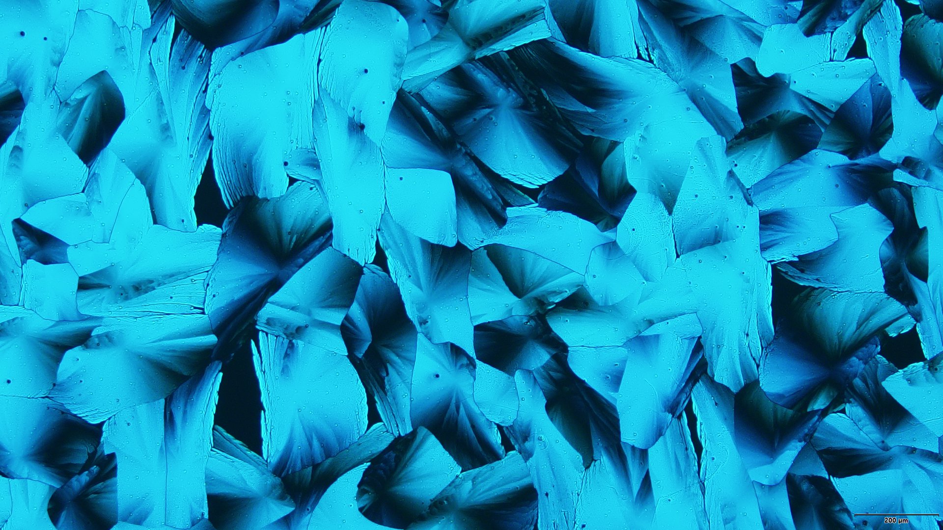
An organic material transitioning from a polycrystalline thin film towards a tangle of three-dimensional elongated crystals. Captured with Olympus BX51 microscope.
An organic field-effect transistor fabricated on a silicon/silicon dioxide substrate, featuring gold source and drain electrodes, and a thin film composed of TIPS-pentacene blended with polystyrene (10k), deposited via the Bar-Assisted Meniscus Shearing (BAMS) technique.
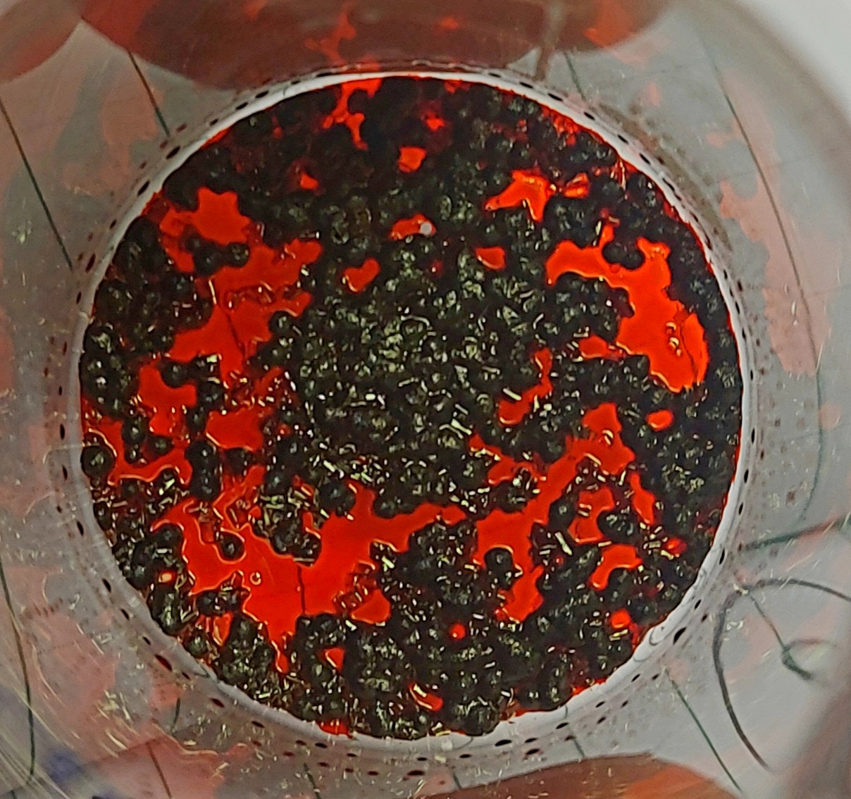
A red dye being purified as a solid where it shows a beautiful morphology!
Fragments of TCNQ scattered across a silicon/silicon dioxide surface, deposited using Bar-Assisted Meniscus Shearing technique.
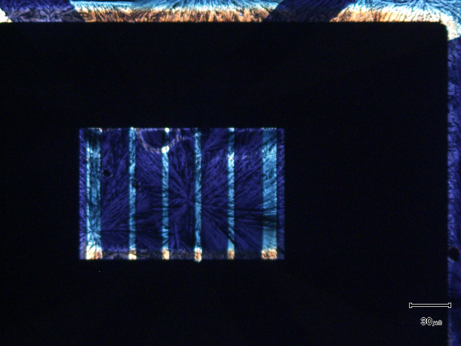
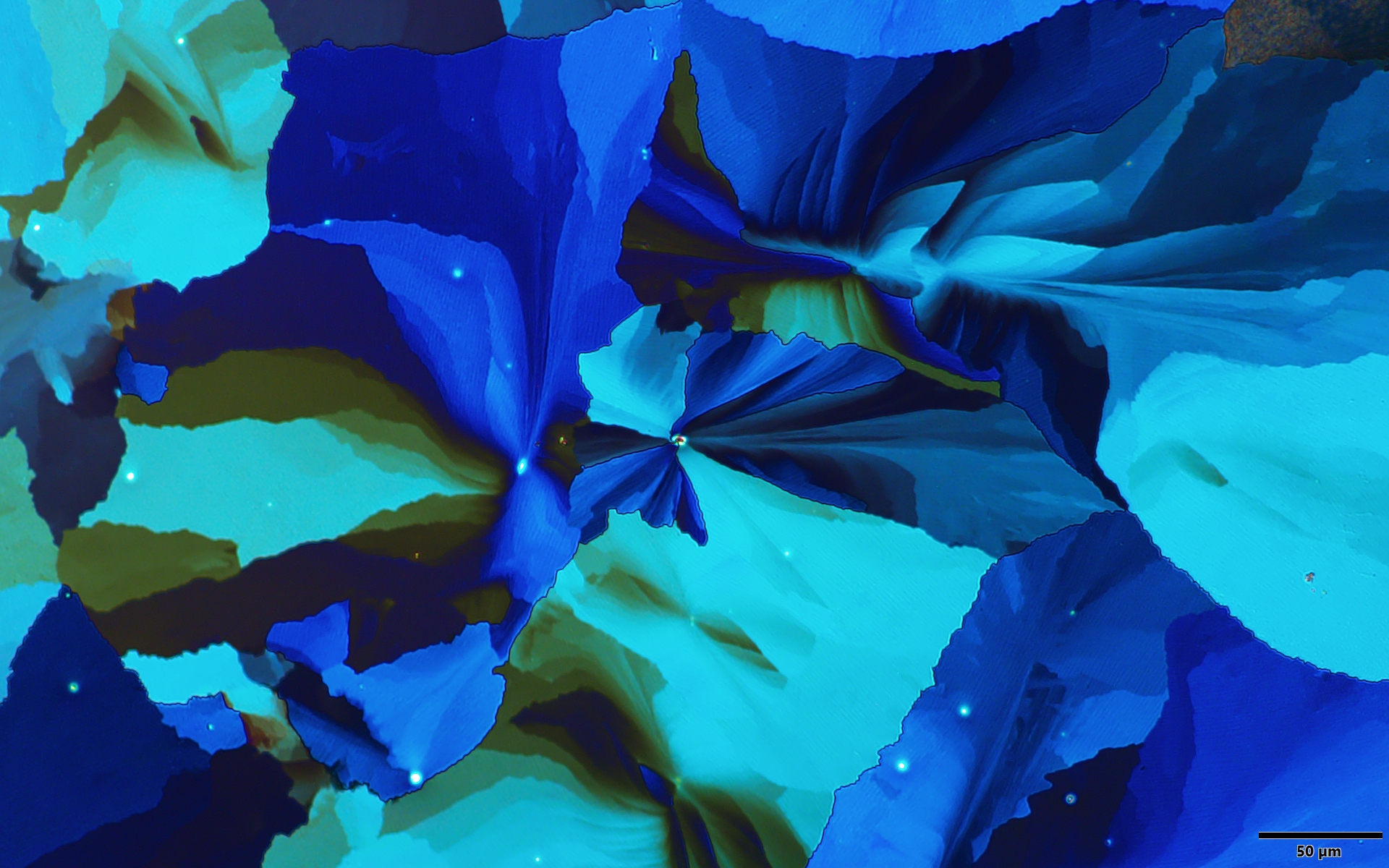
Polarized optical microscopy image of an organic semiconductor thin film.
Thin films of a polymer before (transparent) and after (opaque) annealing.