40 years of materials science
- Picture:
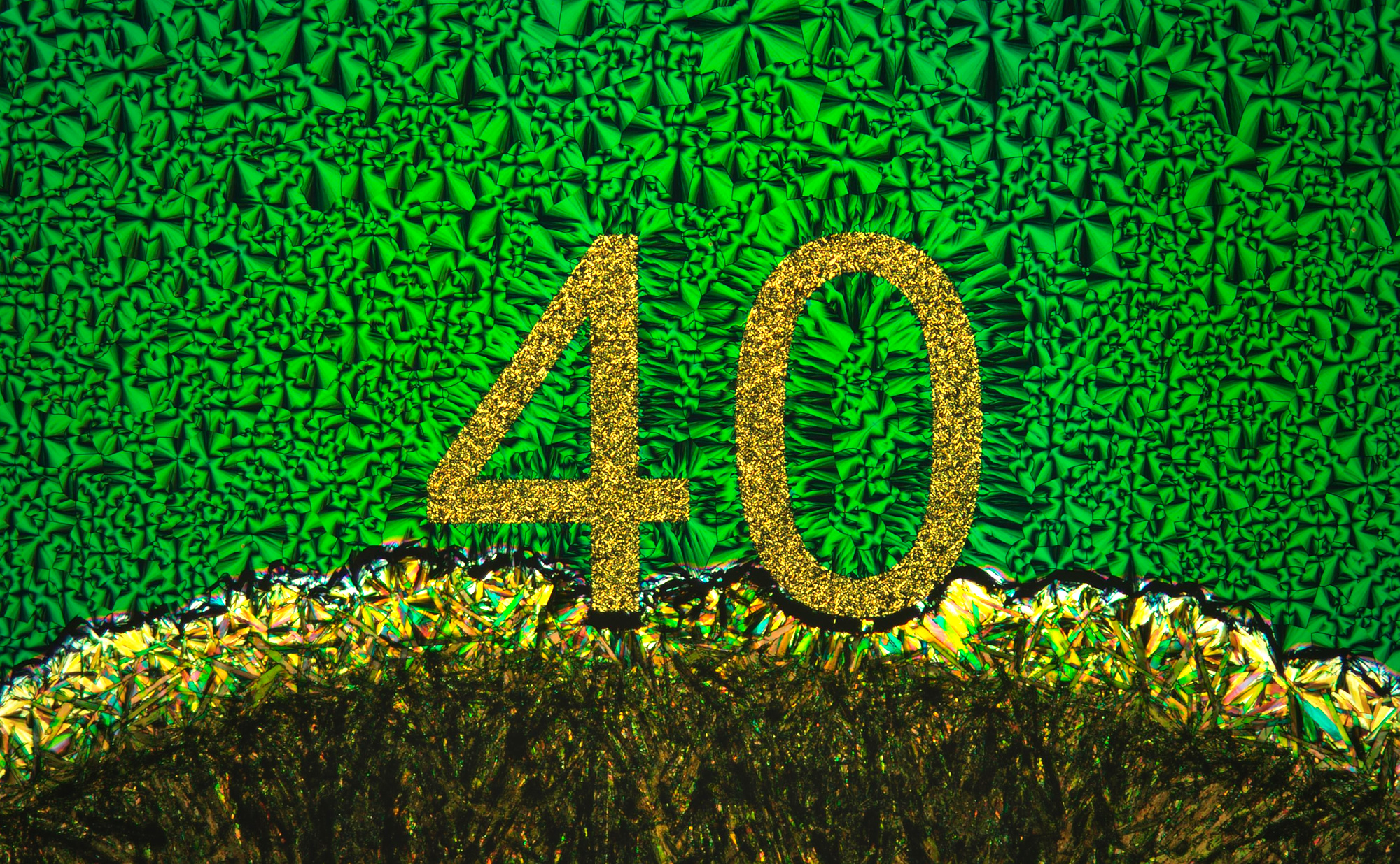
A size label made on the sample by lithography ended up right at the frontier of crystal growth – and happened to match the ICMAB anniversary year! Captured with Olympus BX51 microscope.


A size label made on the sample by lithography ended up right at the frontier of crystal growth – and happened to match the ICMAB anniversary year! Captured with Olympus BX51 microscope.
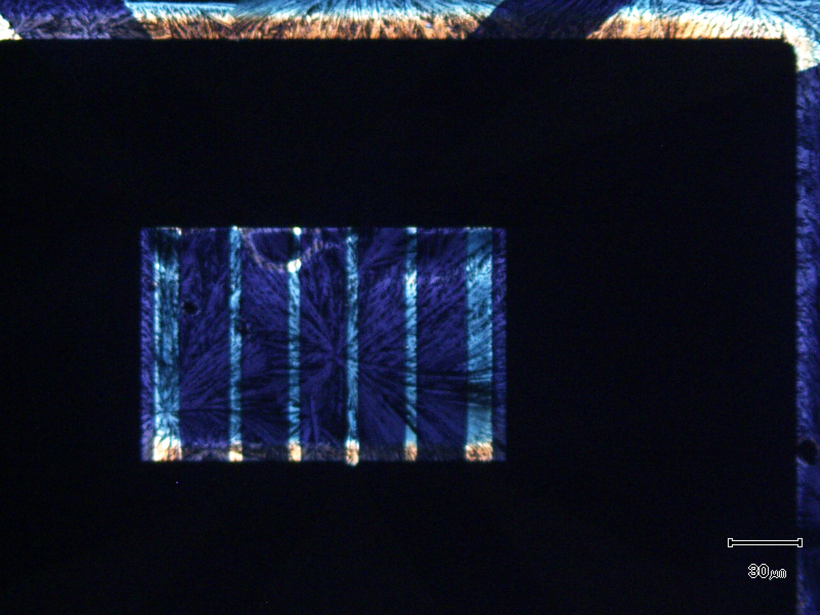
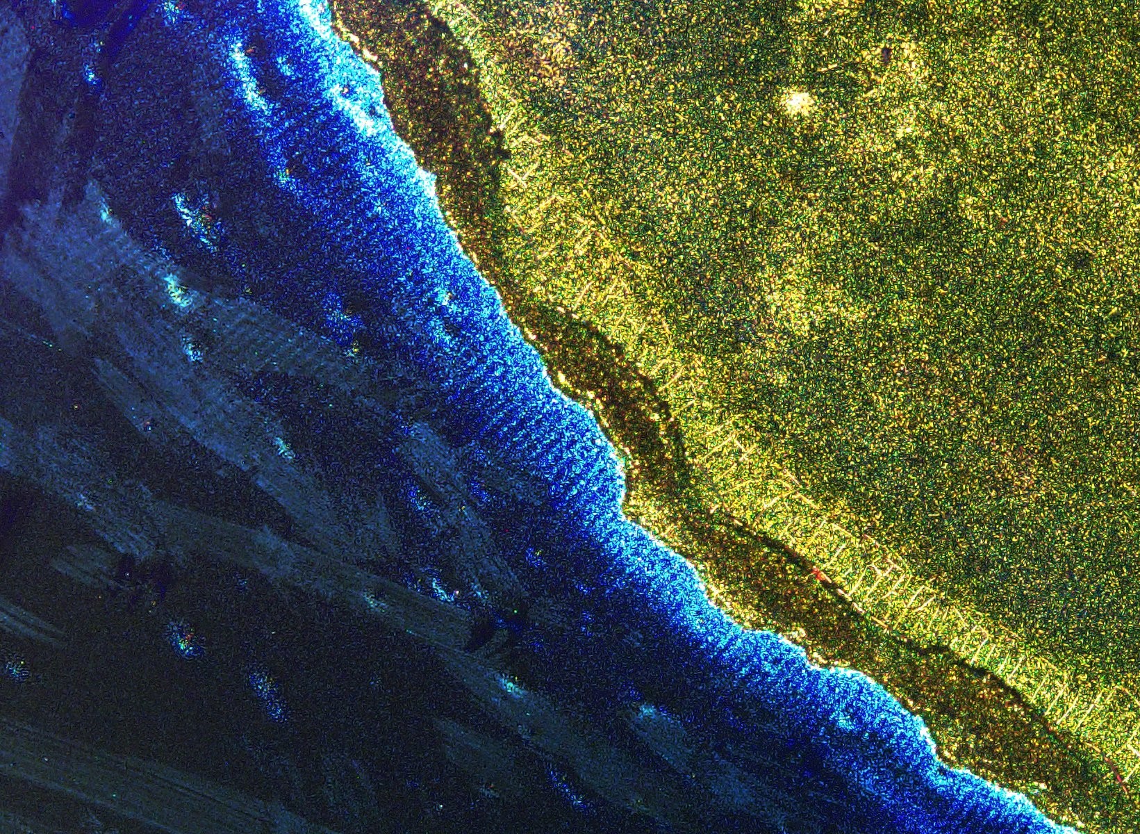
Optical microscopy image of the selective deposition of semiconductor crystals on a chemically modified substrate. The treated regions inhibit crystal growth, while in the transistor channel the semiconductor crystals grow, forming a polycrystalline layer. This contrast between hydrophobic and hydrophilic properties induces a well-defined pattern, relevant for the development of printed electronics, where wettability and capillary forces govern the formation of semiconductor layers.
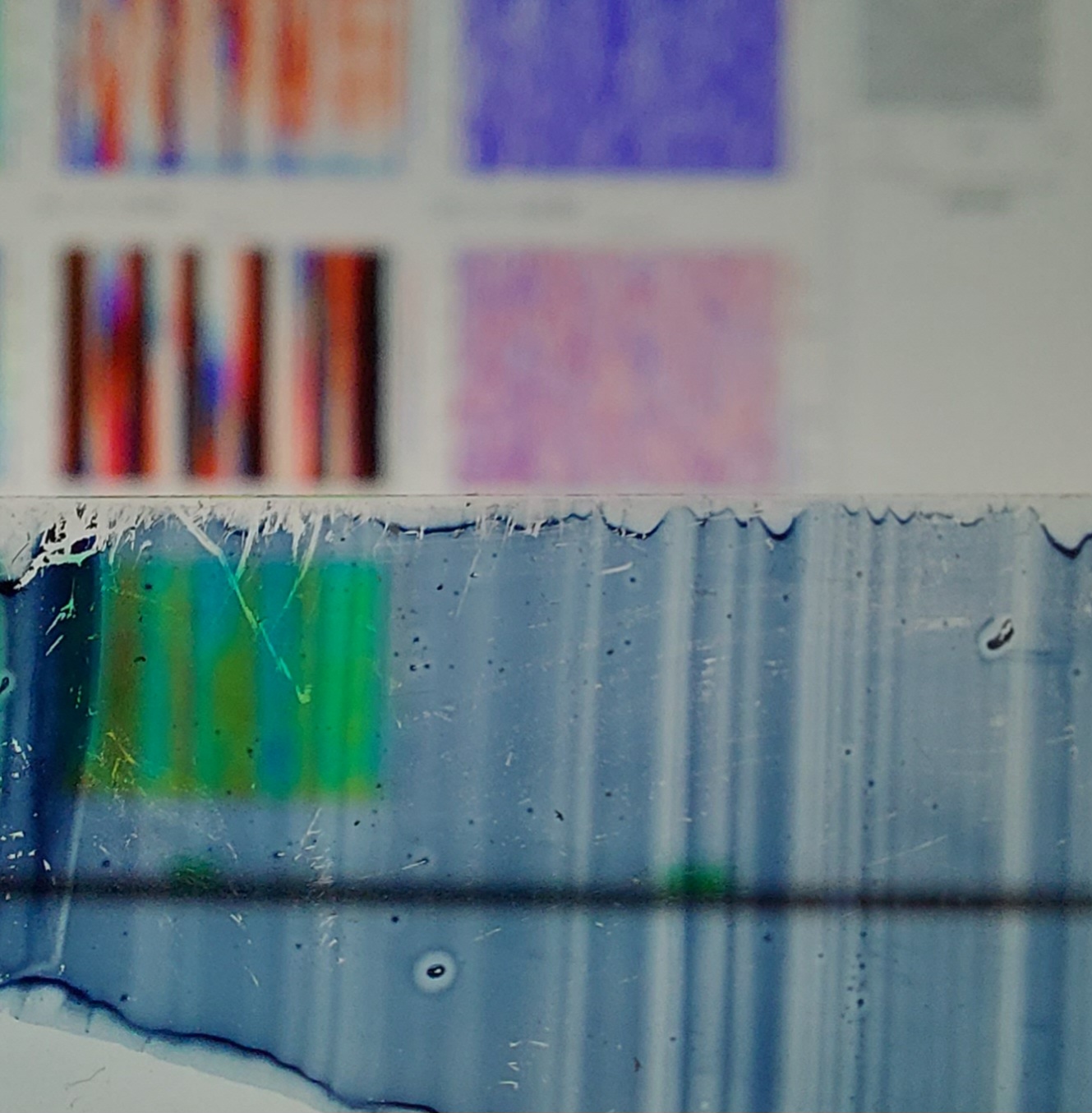
A microscope slide with a sample of an organic material used in solar cells with a spectroscopic image of the sample in the background.
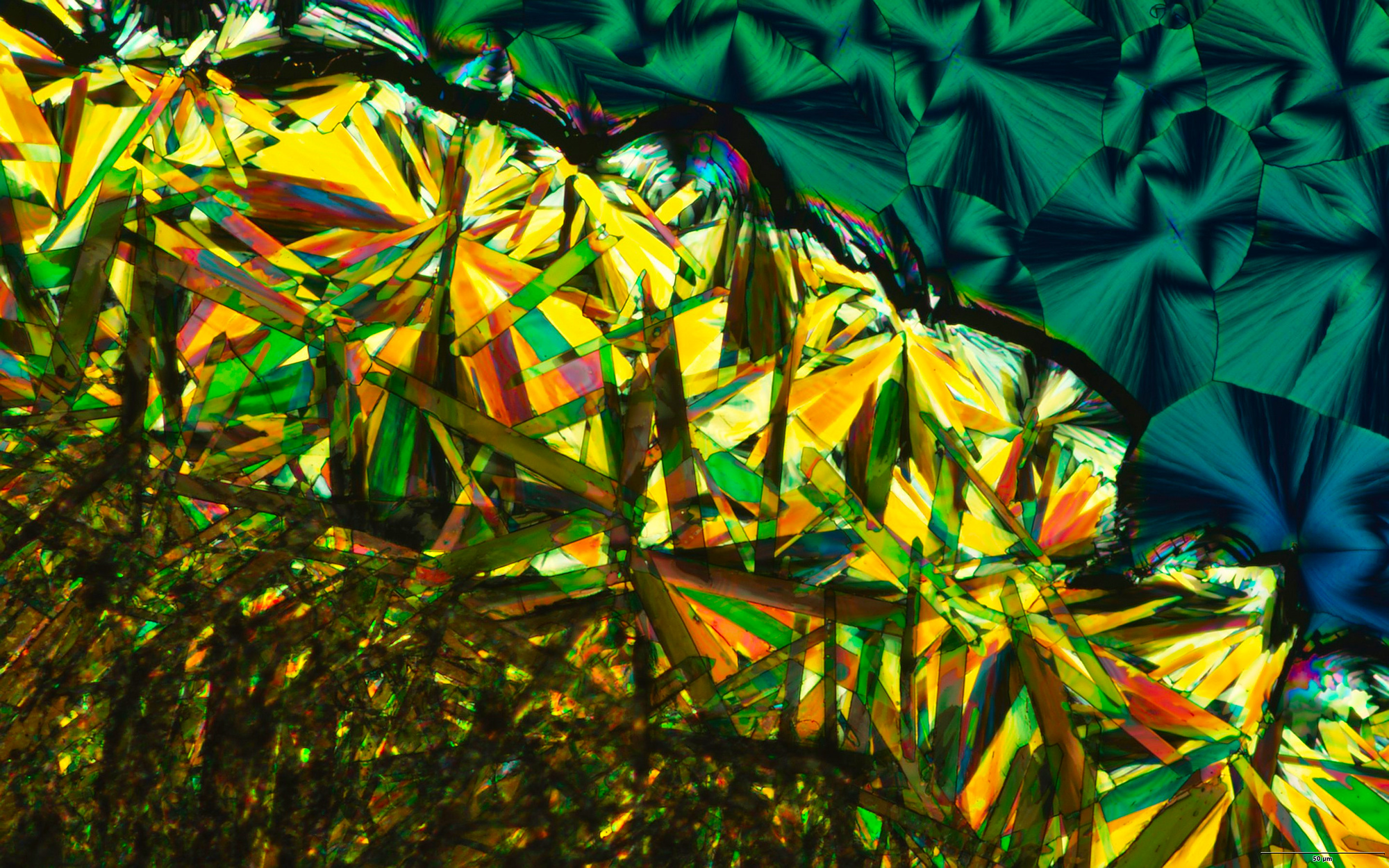
An organic material transitioning from a polycrystalline thin film towards a tangle of three-dimensional elongated crystals. Captured with Olympus BX51 microscope.

An organic field-effect transistor fabricated on a silicon/silicon dioxide substrate, featuring gold source and drain electrodes, and a thin film composed of TIPS-pentacene blended with polystyrene (10k), deposited via the Bar-Assisted Meniscus Shearing (BAMS) technique.
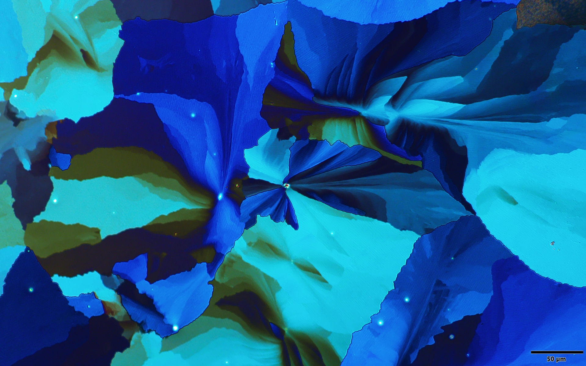
Polarized optical microscopy image of an organic semiconductor thin film.