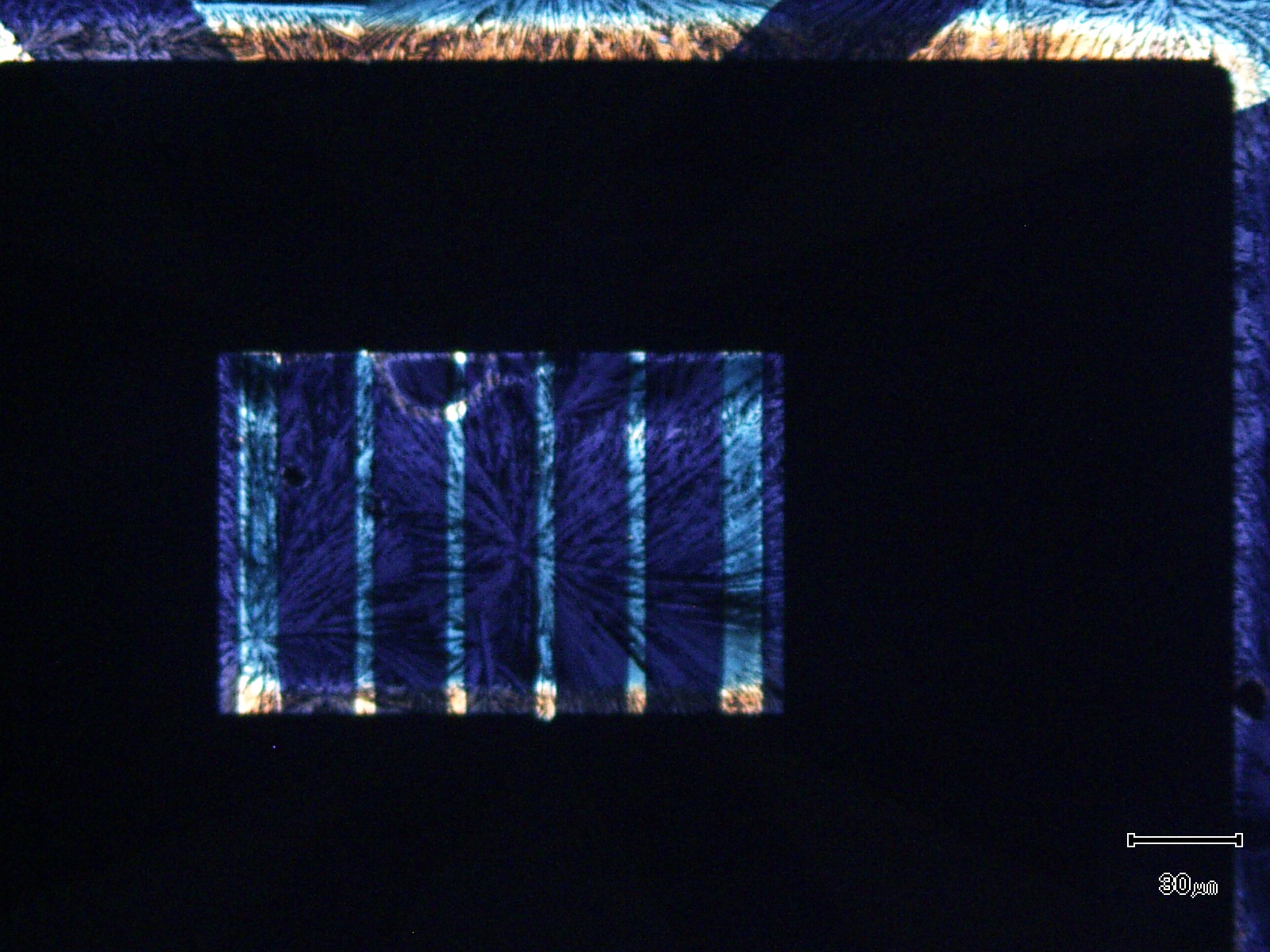
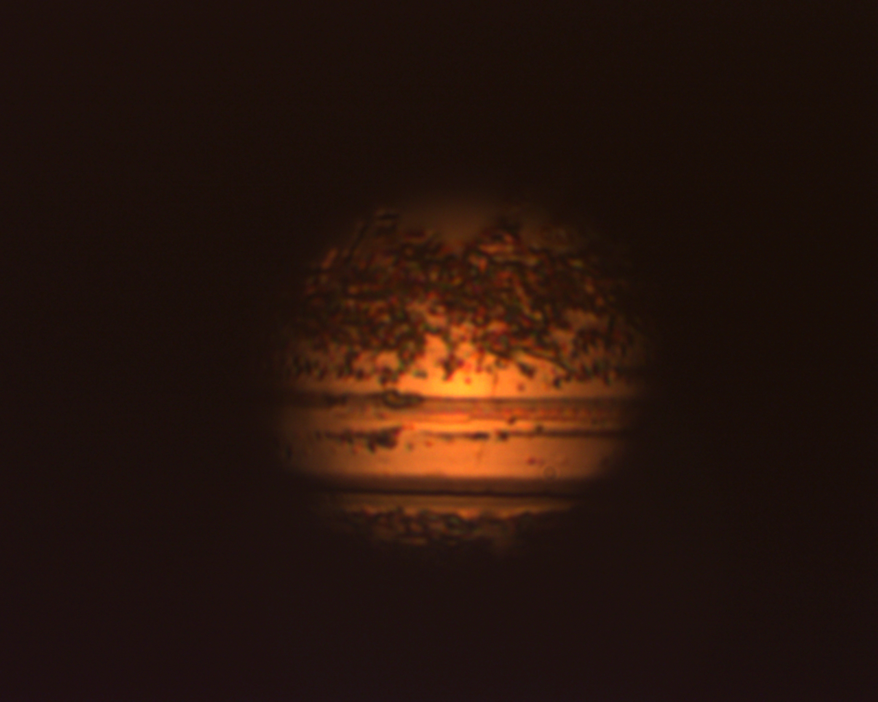
Optical microscopy image of the selective deposition of semiconductor crystals on a chemically modified substrate. The treated regions inhibit crystal growth, while in the transistor channel the semiconductor crystals grow, forming a polycrystalline layer. This contrast between hydrophobic and hydrophilic properties induces a well-defined pattern, relevant for the development of printed electronics, where wettability and capillary forces govern the formation of semiconductor layers.
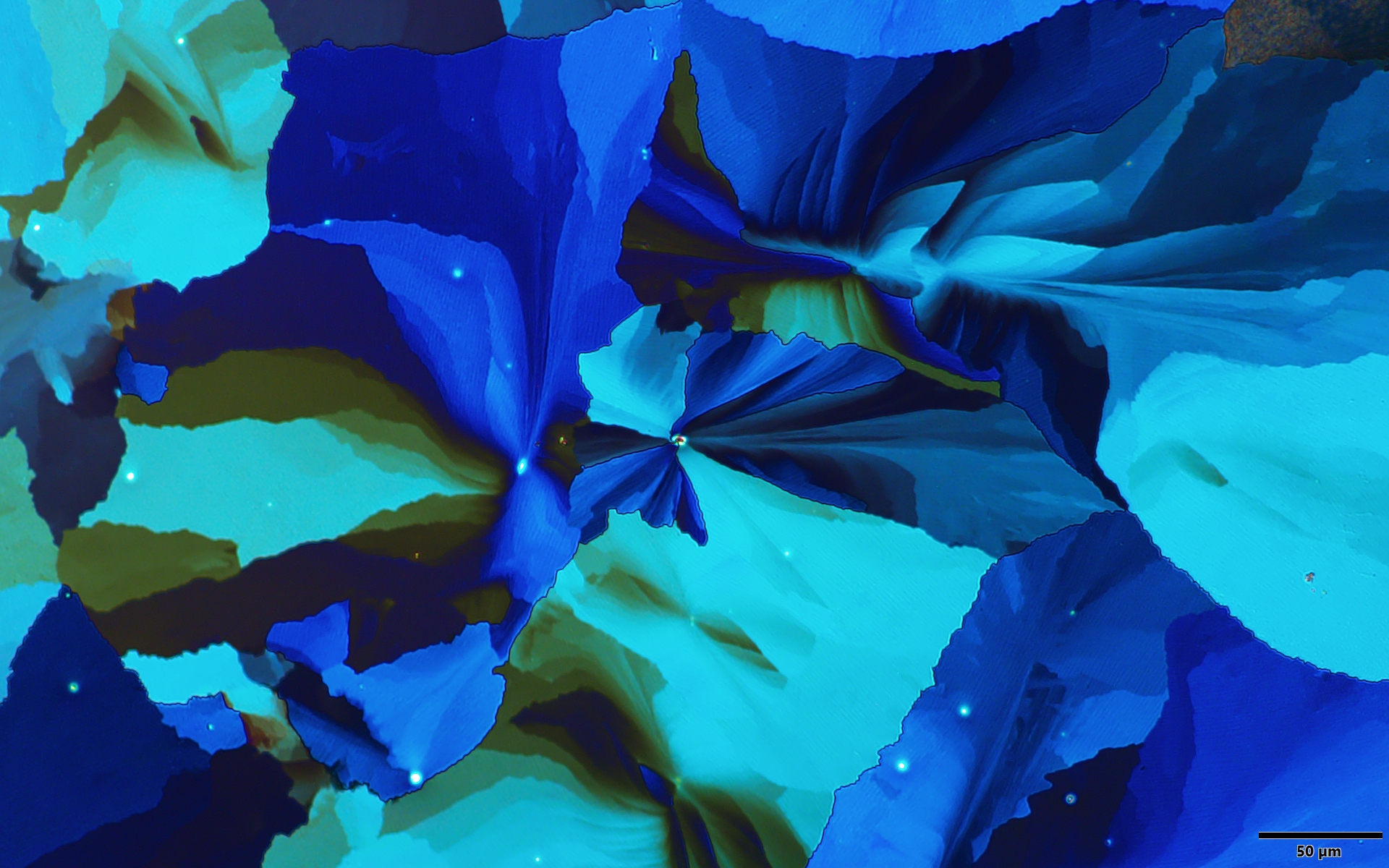
Imagen obtenida con microscopio óptico con luz polarizada que muestra estructuras cristalinas con morfología floral en tonos azules y patrones simétricos formados tras el tratamiento térmico de los films preparados desde disolución.
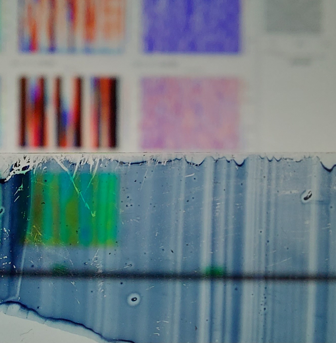
A microscope slide with a sample of an organic material used in solar cells with a spectroscopic image of the sample in the background.
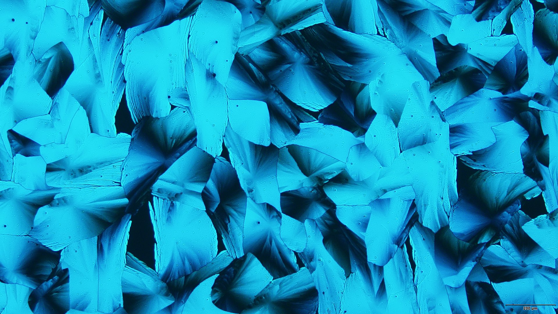
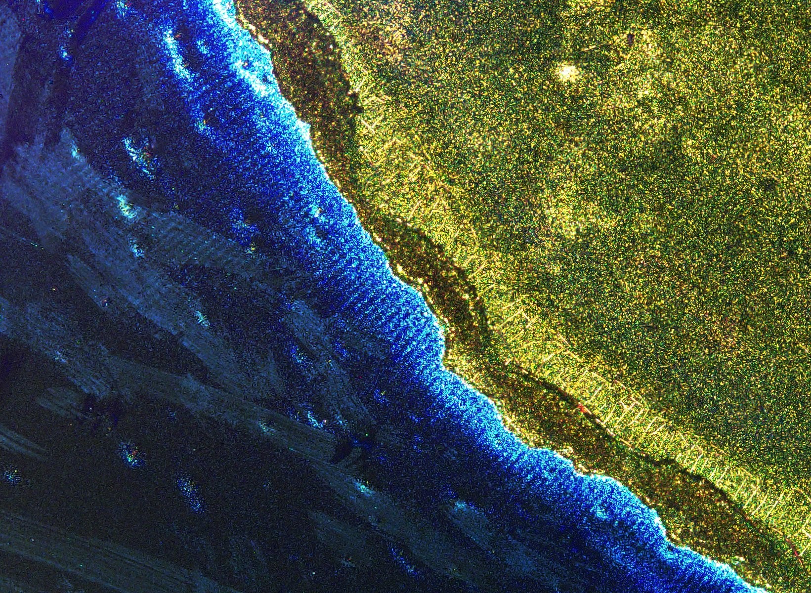
Polarized light microscopy image of a nickel hydroxide film on silicon substrate by spin coating. These striking color patterns are related to changes in the film thickness.
Polarized light microscopy image of a nickel hydroxide film on silicon substrate with cracks formed after thermal treatment.
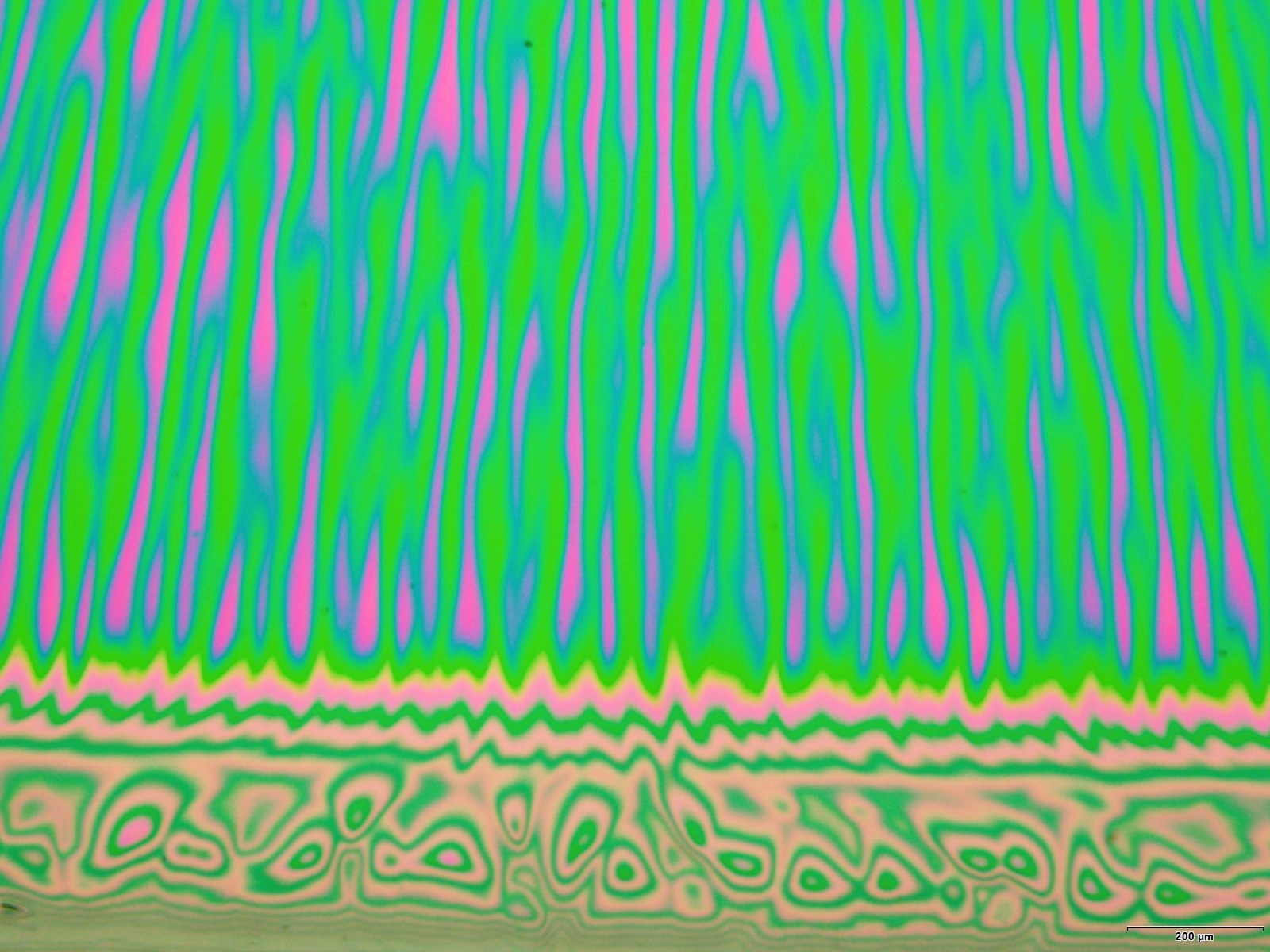
An organic field-effect transistor fabricated on a silicon/silicon dioxide substrate, featuring gold source and drain electrodes, and a thin film composed of TIPS-pentacene blended with polystyrene (10k), deposited via the Bar-Assisted Meniscus Shearing (BAMS) technique.
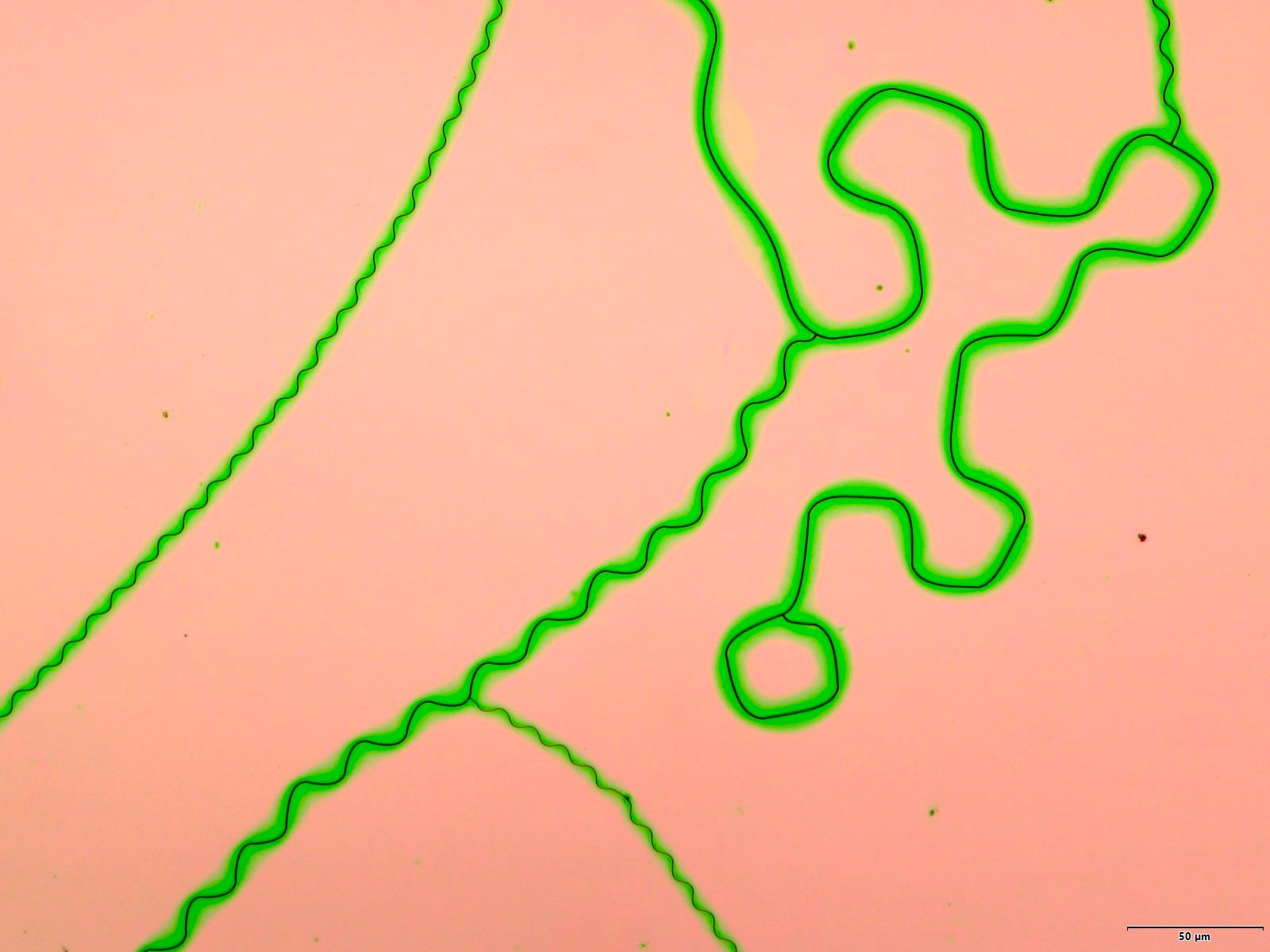
Fragments of TCNQ scattered across a silicon/silicon dioxide surface, deposited using Bar-Assisted Meniscus Shearing technique.
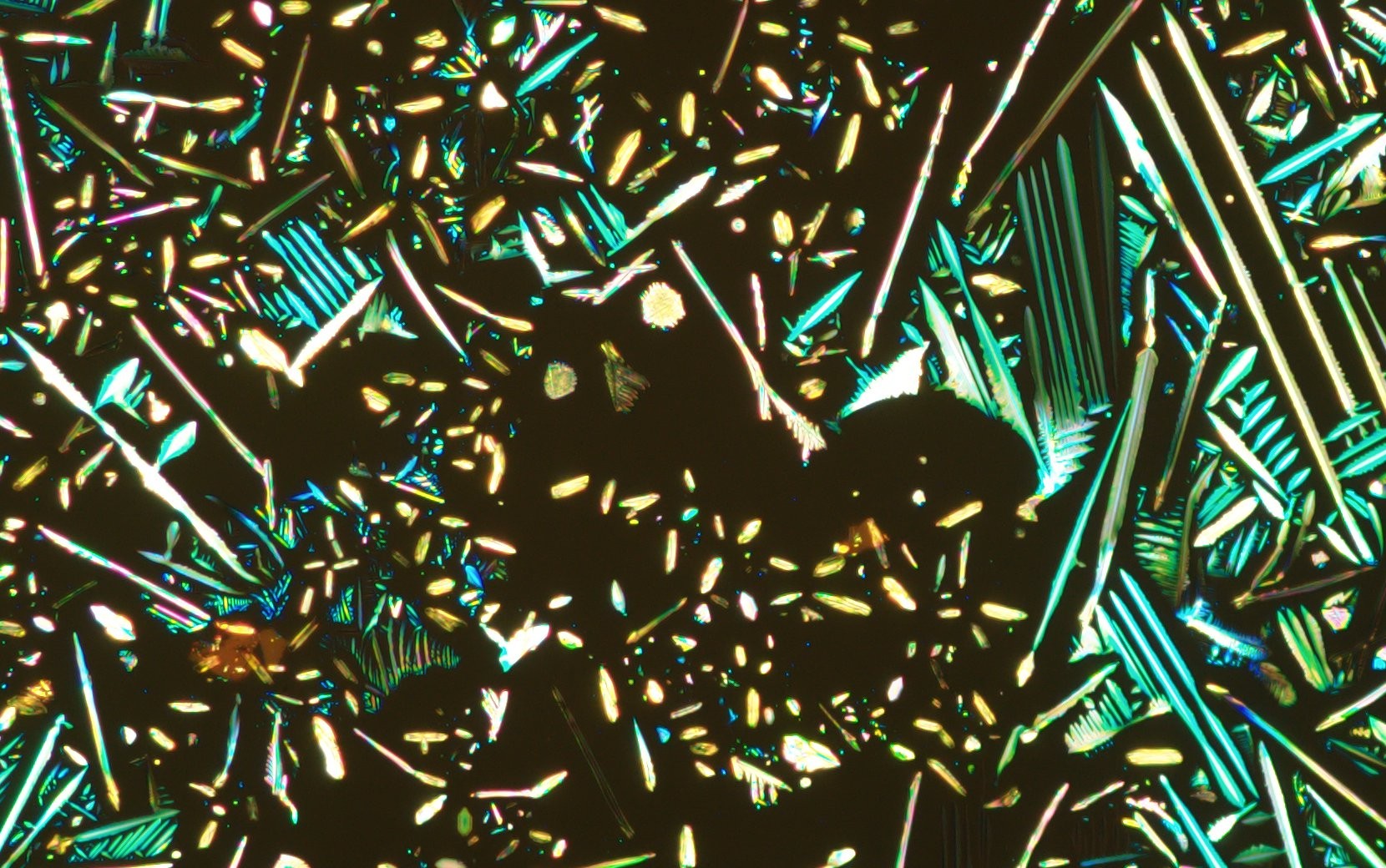
Polarized optical microscopy image of an organic semiconductor thin film.
Fourier microscopy in reflectance. Objective 100x, NA 0.9.
Thin films of a polymer before (transparent) and after (opaque) annealing.