40 years of materials science
- Picture:
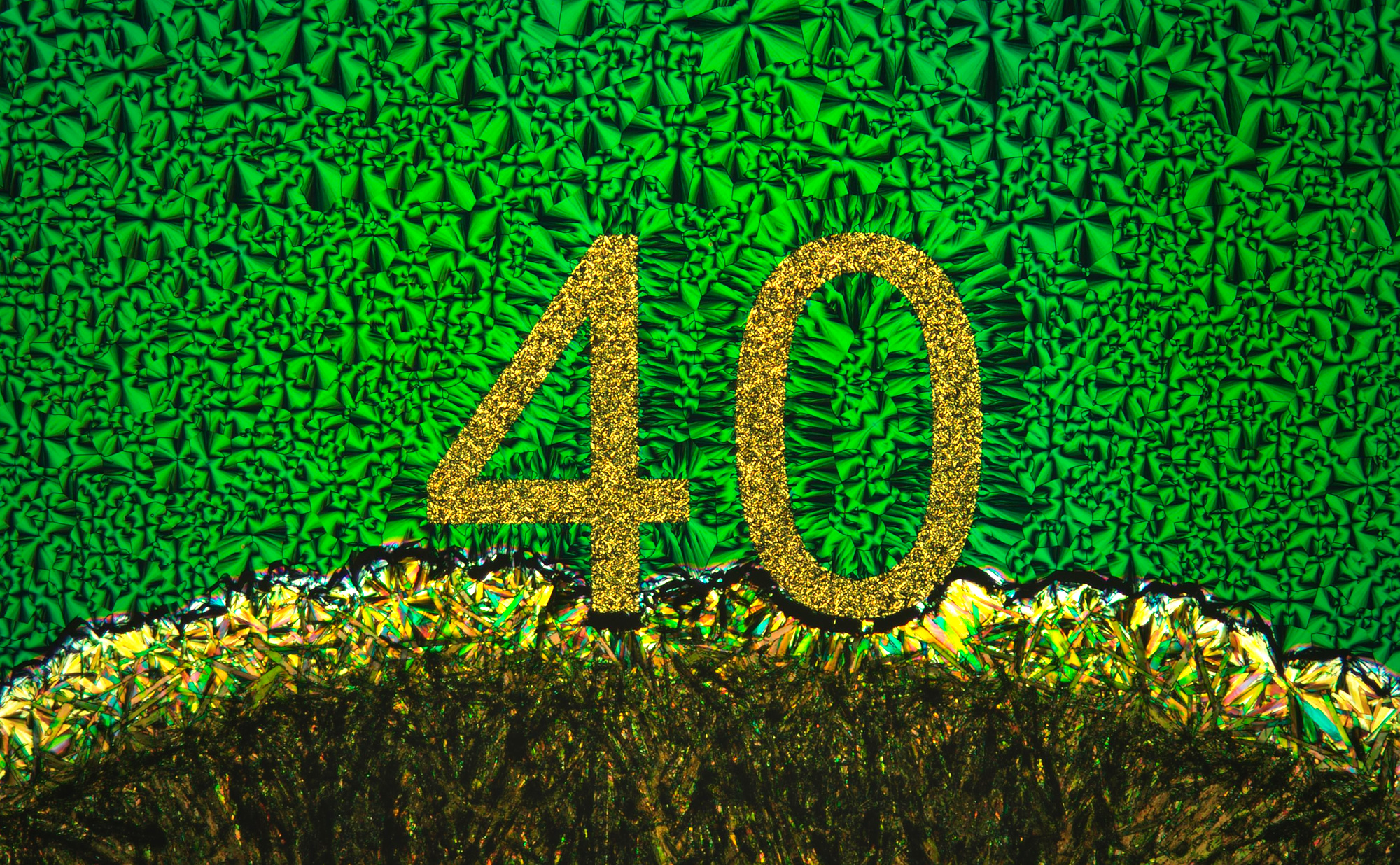
A size label made on the sample by lithography ended up right at the frontier of crystal growth – and happened to match the ICMAB anniversary year! Captured with Olympus BX51 microscope.


A size label made on the sample by lithography ended up right at the frontier of crystal growth – and happened to match the ICMAB anniversary year! Captured with Olympus BX51 microscope.
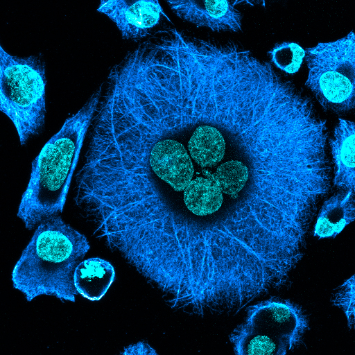
Multinucleated pancreatic cells on a glass slide; intermediate filaments stained with vimentin (blue), cell nuclei stained with Hoechst (cyan).
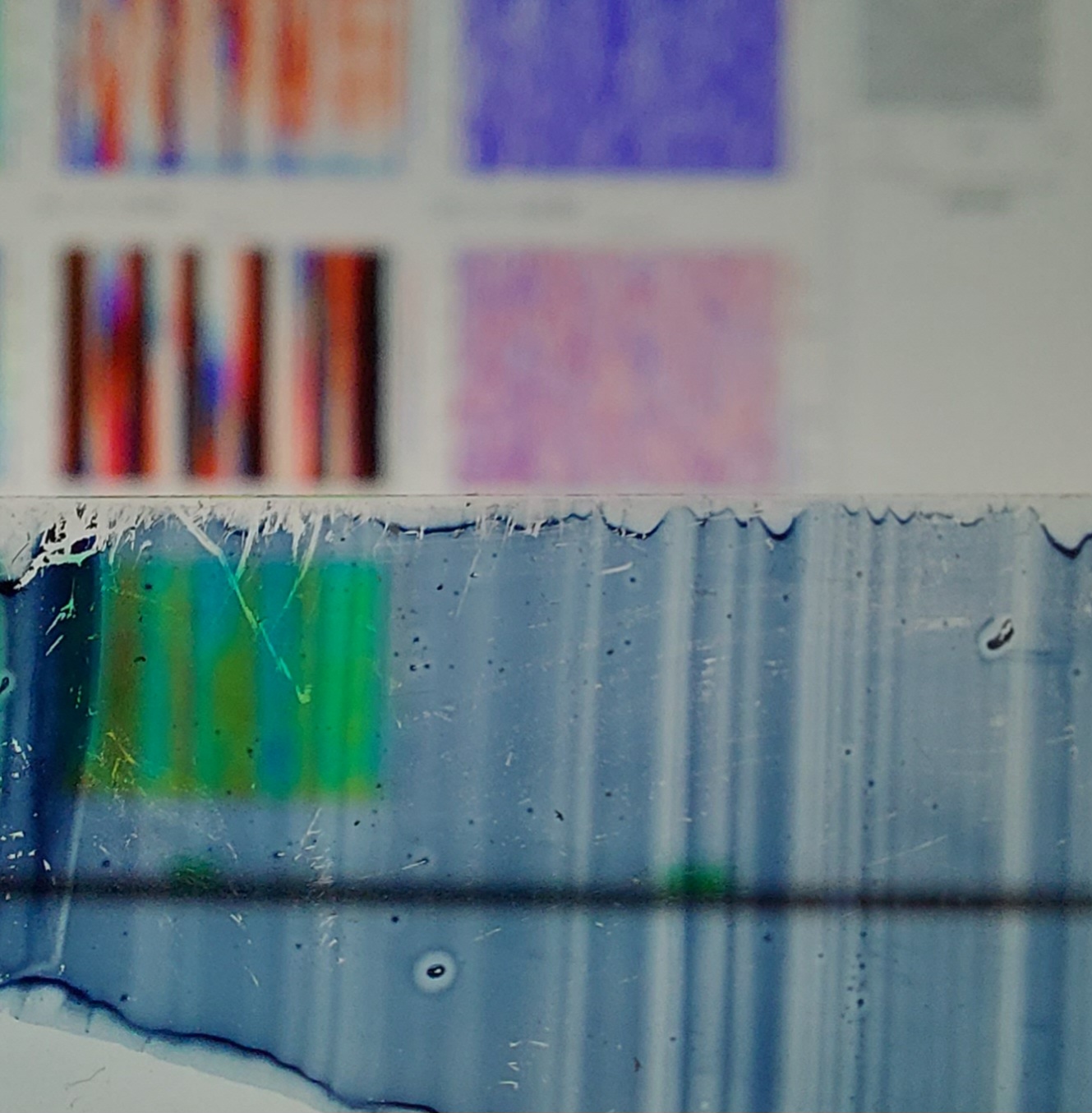
A microscope slide with a sample of an organic material used in solar cells with a spectroscopic image of the sample in the background.
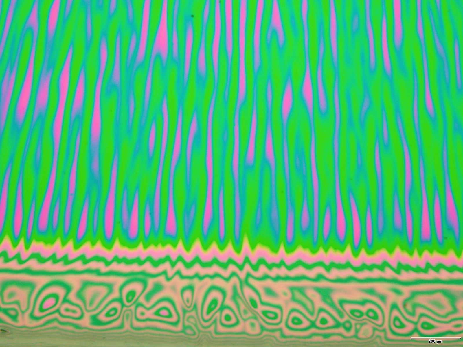
Polarized light microscopy image of a nickel hydroxide film on silicon substrate by spin coating. These striking color patterns are related to changes in the film thickness.
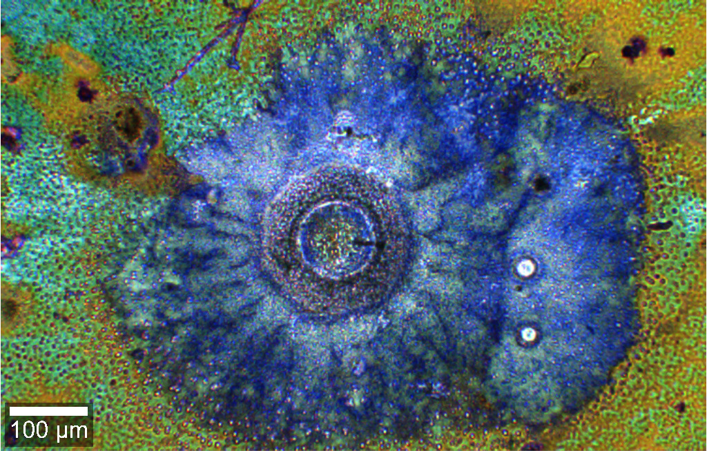
When studying our particle on a mirror system in the Raman set-up, we came across this beautiful volcano resulting from the agglomeration of some nanoparticles.
Polarized light microscopy image of a nickel hydroxide film on silicon substrate with cracks formed after thermal treatment.

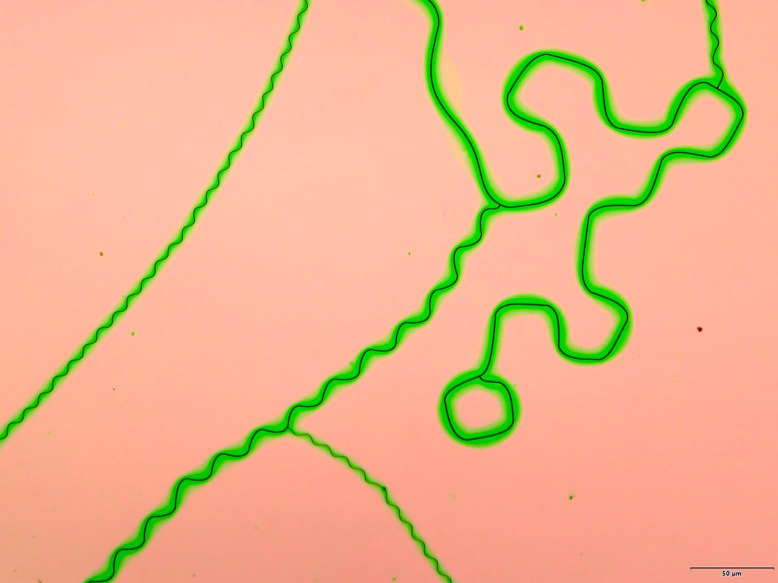
An organic field-effect transistor fabricated on a silicon/silicon dioxide substrate, featuring gold source and drain electrodes, and a thin film composed of TIPS-pentacene blended with polystyrene (10k), deposited via the Bar-Assisted Meniscus Shearing (BAMS) technique.
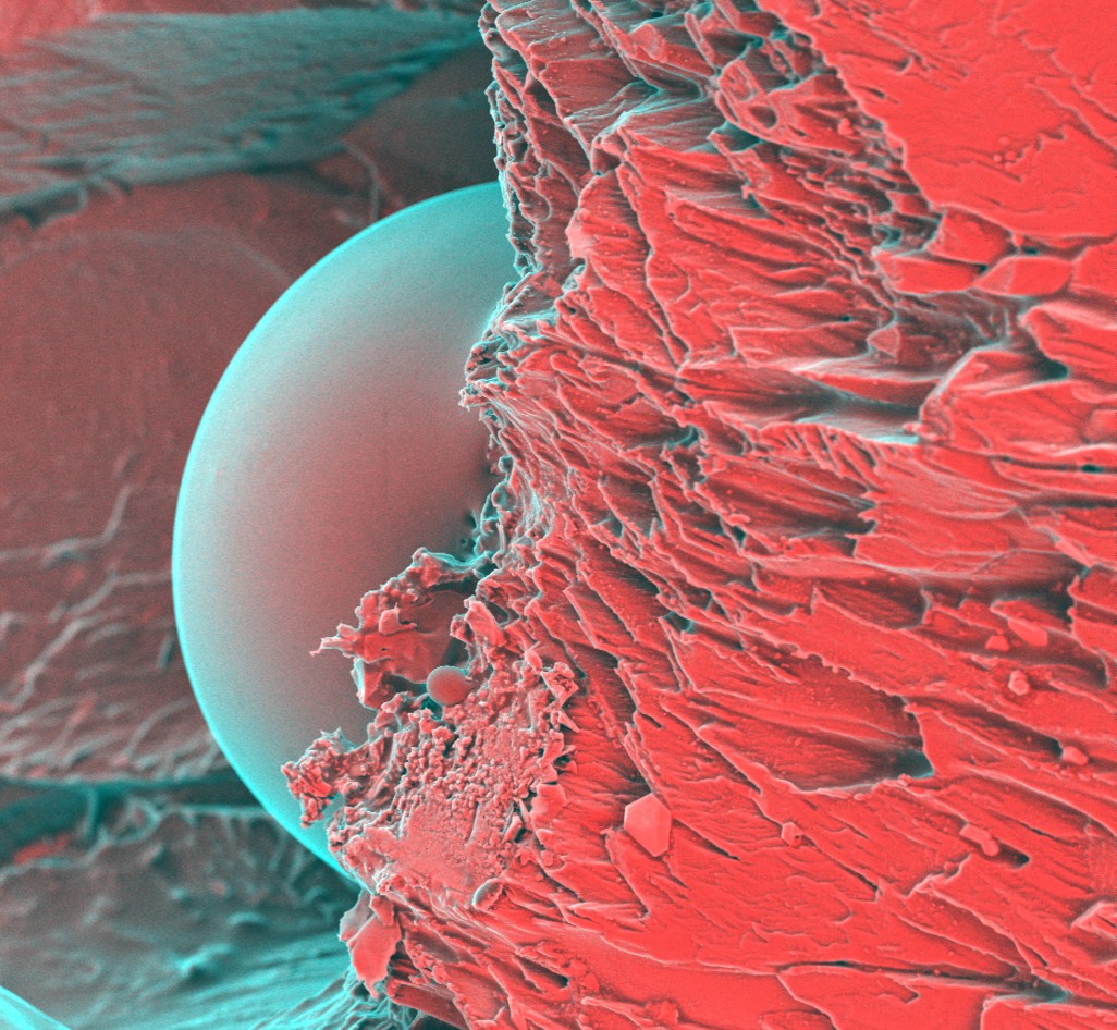
SEM micrograph (QUANTA FEI 200FEG-ESEM) of a mixture of feldspars + quartz, i.e. a silicate-rich rock (granite/granodiorite type).

In 1675, Isaac Newton wrote, “If I have seen further, it is by standing on the shoulders of giants.” Through the lens of the microscope, science finds its vision, revealing the intricate details of a world otherwise invisible. Perhaps, sometimes, becoming giants begins with learning to see the smallest, microscopic, things.